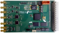
Hardware/FPGARackADDAV1
From UIT
|
Warning : This board is deprecated. See HiRADDA and HiSADDA boards.
The main purpose behind this board is to have a powerful development FPGA board specialized in data acquisition and processing. The stock can be verified and updated on-line.
| Type | FPGA Rack | Documentation | Description |
|---|---|---|---|
| V1.0 |  |
OLGMADDA V1.0 UCF File Full documentation |
Spartan6 XC6SLX45 |
The boards are compatible with the FPGA Rack Backplane for interconnecting different boards with the help of the HEI Backplane Bus and the HES-SO VME IP Core.
Features
- 2x A/D 24bits 2.5MSPS (Analog Devices AD7760)
- 2x A/D 16bits 10MSPS (Analog Devices AD7626)
- 1x D/A 16bits with 4MHz bandwidth - Two Channels (Analog Devices AD5547)
- 1x Xilinx Spartan6 LX45
- 1-2x Xilinx Platform Flash (min. 16MBit required)
- 1x JTAG Connector
- 1x UART (DIL Connector)
- 1x Trigger input
- 1x VME Compatible Connector 3x32 pins
- 6x LEDs
- 8x DIL Switches
- 1x 100MHz Quartz for main clock
- Powered by VME Connector or a specific power connector
VME connector logic levels
The I/O bank which interfaces the VME connector can be powered with 3.3V or with 2.5V. A zero-Ohm resistor has to be soldered at the proper place near the FPGA.
Programmation
This board can be programmed in 2 ways,
- First the FPGA can be directly programmed.
- Second the FPGA can be programmed via the onboard Flash memory.
For more explanation see at the Howto below:
Links
- Xilinx Spartan 6 Documents
- VME Connector Description
Known issues
The following points need to be corrected for a newer version of the board :
- Digital I/O of AD7xxx are compatible 2.5V (and not 3.3V). Banks reorganisation needed.
- If bank #1 is 2.5V for avoid destroying the AD7760, the UART chip can't be used (Voltage Input Threshold of 2.4V...).
- Better routage of the 250MHz LVDS lines (shielding and distance).
- Better placement of the SMA connectors with possibility to add a front bracket.
- Modify Xilinx FLASH core voltage to 1.8V.
- Add a 1.8V power supply for Xilinx FLASH.
- ...or replace theses 50$ FLASH with a small standard 2$ FLASH.
- Move the FPGA core power supply (1.2V) from the LDO to a DC/DC power supply.
- Distance the RS232 DIL connector from the JTAG connector.
- Use a bigger / with better speed grade FPGA ?