Hardware/FPGARackHiSADDAV1
|
Not up to date, content will be refreshed soon...
The main purpose behind this board is to have a powerful development FPGA board specialized in data acquisition and processing, like the FPGA Rack AD/DA V1 but at high frequency. This board was developped as a part of the gal's (Alexandre Ganchinho) master thesis.
| Type | FPGA Rack | Documentation | Description |
|---|---|---|---|
| V1.0 |  |
Full documentation |
Kintex7 XC7K160T-2FFG676 |
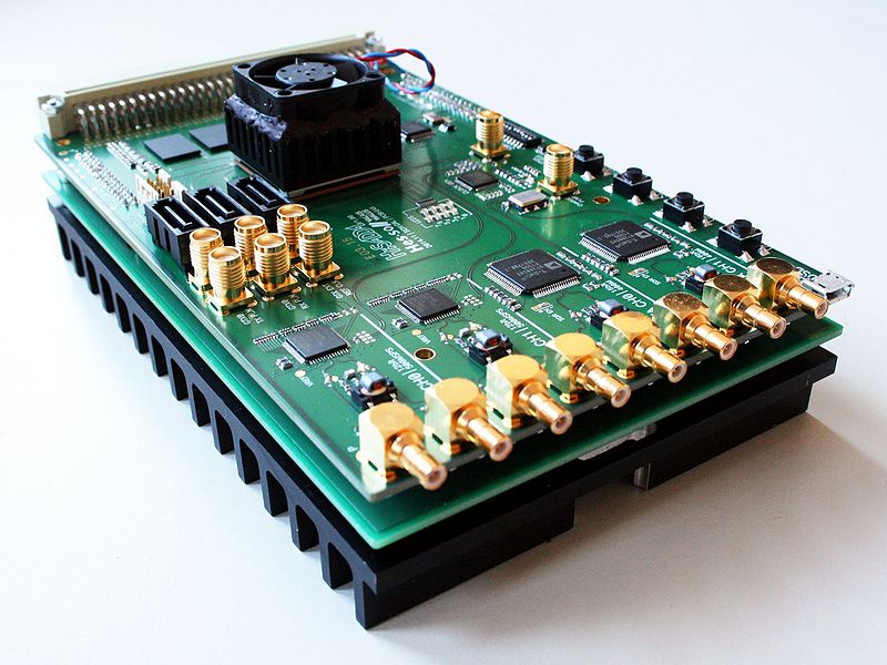
The HiSADDA set is composed of two board : HiSADDA Core and HiSADDA Power.
HiSADDA is compatible with the FPGA Rack Backplane for interconnecting different boards with the help of the HVME16 version of the HES-SO Backplane Bus and the HES-SO VME IP Core.
Core features
- 2x A/D 12bits 500MSPS (Analog Devices AD9434-500) with 3 analog paths :
- Direct (differential - BW DC..1GHz)
- Through balun (single ended / differential - BW 5..200MHz)
- Through operationnal amplifier (single ended to diff. conversion, Max BW DC..320MHz)
- 2x D/A 16bits 400MSPS (Analog Devices AD9726), current source, with 2 analog paths :
- Direct (differential - BW DC..200MHz)
- Through balun (single ended / differential - BW 5..200MHz)
- 1x Xilinx Kintex7 XC7K160T-2FFG676
- 162.24k logic cells, 25.35k slices (max 2.188Mb of distributed RAM)
- 11.7Mb block RAM (650x18Kb / 325x36Kb)
- 600 DSP Slices
- GTX
- 2x DDR3 (total: 1GiB, 32bit width)
- 2x 32MiB Serial QuadSPI NOR Flash (one reserved for FPGA programming)
- 1x USB2 (micro USB connector, FTDI FT232HL)
- 3x SATA connector (for general purpose gigabit link - expermiental)
- 1x SMA connectors set for general purpose gigabit link (1 lane per RX/TX - Xilinx dev. kit compatible)
- 1x DIN41612 VME Compatible Connector 3x32 pins (only HVME16) with CMOS AC termination on all signal pins (unsoldered - expermiental)
- 1x Low-jitter clock generator/distributor for FPGA core, ADs, DAs and DDR3 (Analog Devices AD9517-4)
- 1x additionnal 100MHz quartz for boot clock
- 8x user LEDs
- 10x user DIL Switches
- 1x JTAG Connector
- 1x power supply card connector (mandatory)
Power supply considerations
The HiSADDA Core board has no DC/DC nor LDO chip and is only powered with a dedicated power supply card (for PCB placment constraints and thermal considerations). External power supplies needed : +12V Digital (6..20V tolerant), +/-5V Analog. It must be plugged with the HiSADDA Power board.
Please note that this board can't be powered though the DIN41612 connector (power pins intentionnaly left unrouted).
The absolute maximum power consumption of the board itself is calculated around 22.5W. At this power, thermal losses in the power supply card is predicted around 18W. Estimated total consumption for normal use is planned around 10-40W - heavily depending on used functionnalities. Active dissipation can be needed (mandatory in a rack - the FPGA fan starts when plugged in a backplane).
VME connector logic levels
The I/O bank which interfaces the VME connector is only 3.3V. Be careful with other FPGA Rack boards with 2.5V/3.3V jumper.
Programming
The FPGA on this board can be programmed in 2 ways :
- directly through JTAG interface.
- automatically on boot via the onboard FLASH memory (SPI x1/x4).
More explanation about FLASH programming are available here.
Validated features
This board is quite young, so not all features have been fully tested yet. Here's a list of operational feature :
- OK Power stability. (NB: Issues can occurs on high FPGA core current demand because of voltage drop due to resistive losses on PCB)
- OK FPGA boot FLASH programming/booting (with SPI 1x and 4x).
- OK Boot clock on FPGA.
- OK Users misc I/Os (buttons, switches, LEDs).
- OK USB<->FIFO245 FTDI.
- OK AD9517-4 with 1.6GHz VCO or external clock - fully configurated via SPI using OLGMCLNT V2 PC client.
The following points will be tested soon :
- TODO ADCs and DACs.
- TODO DDR3 SDRAM.
The following point will be tested depending on projects demand :
- IDLE Second FLASH IC.
- IDLE Gigabit I/Os (SATA and SMA).
Known issues
- 0402 100Ohms LVDS termination resistors must be added under the FPGA between pins E18-D18 and H17-H18 in order to use the DDR3 chips. If not used, the outputs DDR3-FPGA_CLK0P/N and DDR3-FPGA_CLK1P/N from the AD9517-4 must be disabled.
- Decoupling capacitors missing on bank 32. It is recommanded to add manually 100uF + 47uF (X5R/X7R).

