Hardware/FPGARack
m |
|||
| (14 intermediate revisions by 5 users not shown) | |||
| Line 1: | Line 1: | ||
{{TOC right}} | {{TOC right}} | ||
| − | The basic idea behind this board is to have a development FPGA board, with a choice of big FPGA's and a VME compatible 2U Rack connector. | + | The basic idea behind this board is to have a development FPGA board, with a choice of big FPGA's and a VME compatible 2U Rack connector. The [[Hardware/Stock_FPGA-Rack|stock]] can be verified and updated on-line. |
{|class=wikitable | {|class=wikitable | ||
| Line 7: | Line 7: | ||
! Type || FPGA Rack || Schematic || UCF || Description | ! Type || FPGA Rack || Schematic || UCF || Description | ||
|- | |- | ||
| − | | V1.0 || [[File:FPGA_Rack_v1_0.jpg|200px|FPGA Rack V1.0]] || [[Media:FPGARack_v1_0_schematics.pdf|FPGA-Rack v1.0 Schematic PDF]] || [[Media:FPGARack_v1_0.ucf|FPGA-Rack v1.0 UCF Files]] || There are different FPGA mounted: Spartan 6 XC6SLX45, Spartan 6 XC6SLX100, Spartan 6 XC6SLX150 | + | | V1.0 || [[File:FPGA_Rack_v1_0.jpg|200px|FPGA Rack V1.0]] || [[Media:FPGARack_v1_0_schematics.pdf|FPGA-Rack v1.0 Schematic PDF]] || [[Media:FPGARack_v1_0.ucf|FPGA-Rack v1.0 UCF Files]] || There are different FPGA mounted: Spartan 6 XC6SLX45, Spartan 6 XC6SLX100, Spartan 6 XC6SLX150 |
|- | |- | ||
|} | |} | ||
| + | |||
| + | The boards are compatible with the [[Hardware/FPGARackBackplane|FPGA Rack Backplane]] for interconnecting different boards with the help of the [[Standards/HEI_'VME'_Backplane_Bus|HES-SO Backplane Bus]] and the [[Components/IP/VME|HES-SO VME IP Core]]. | ||
A VHDL test code with the default UCF Files can be found at the EDA SVN Repository: | A VHDL test code with the default UCF Files can be found at the EDA SVN Repository: | ||
| − | * https://repos.hevs.ch/svn/eda/VHDL/ | + | * https://repos.hevs.ch/svn/eda/VHDL/fgpa_rack |
= Limitation = | = Limitation = | ||
| − | There are Boards with 3 types of FPGA's on it; XC6SLX45, XC6SLX100 and XC6SLX150. | + | There are Boards with 3 types of FPGA's on it; ''XC6SLX45'', ''XC6SLX100'' and ''XC6SLX150''. |
| + | {{WarningBox|content=Mezzanine Pin <code>T8</code> - <code>MEZ_PB19</code> can't be used if a ''XC6SLX100'' is mounted.}} | ||
| − | There | + | = Leds and Buttons = |
| + | There are 4 Dil switches and 4 Leds mounted on the FPGARack board. They are not properly indicated 0 - 3 therefore see the image below. | ||
| − | + | [[File:FPGA_Rack_v1_0_LedsButtons.jpg|200px|FPGA Rack V1.0 Leds and Buttons]] | |
= Features = | = Features = | ||
| − | * 2 Port Ethernet | + | * 2 Port Ethernet (one PTP physical) |
* USB FTDI | * USB FTDI | ||
* 2 UART | * 2 UART | ||
| Line 37: | Line 41: | ||
* Powered by USB or VME Power | * Powered by USB or VME Power | ||
| + | = VME connector logic levels = | ||
| + | The I/O bank which interfaces the VME connector | ||
| + | (and the little black connectors) | ||
| + | can be powered with 3.3V or with 2.5V. | ||
| + | A zero-Ohm resistor has to be soldered at the proper place near the FPGA. | ||
= Programmation = | = Programmation = | ||
| Line 48: | Line 57: | ||
= Links = | = Links = | ||
* [http://www.xilinx.com/support/documentation/spartan-6.htm Xilinx Spartan 6 Documents] | * [http://www.xilinx.com/support/documentation/spartan-6.htm Xilinx Spartan 6 Documents] | ||
| − | * [ | + | * [[Standards/VME|VME Description]] |
| − | + | ||
| − | + | ||
| − | + | ||
[[File:fpga_rack_system.png|FPGA Rack System]] | [[File:fpga_rack_system.png|FPGA Rack System]] | ||
[[Category:Hardware]] [[Category:FPGARack]] | [[Category:Hardware]] [[Category:FPGARack]] | ||
Latest revision as of 14:08, 5 April 2017
|
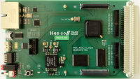
The basic idea behind this board is to have a development FPGA board, with a choice of big FPGA's and a VME compatible 2U Rack connector. The stock can be verified and updated on-line.
| Type | FPGA Rack | Schematic | UCF | Description |
|---|---|---|---|---|
| V1.0 |  |
FPGA-Rack v1.0 Schematic PDF | FPGA-Rack v1.0 UCF Files | There are different FPGA mounted: Spartan 6 XC6SLX45, Spartan 6 XC6SLX100, Spartan 6 XC6SLX150 |
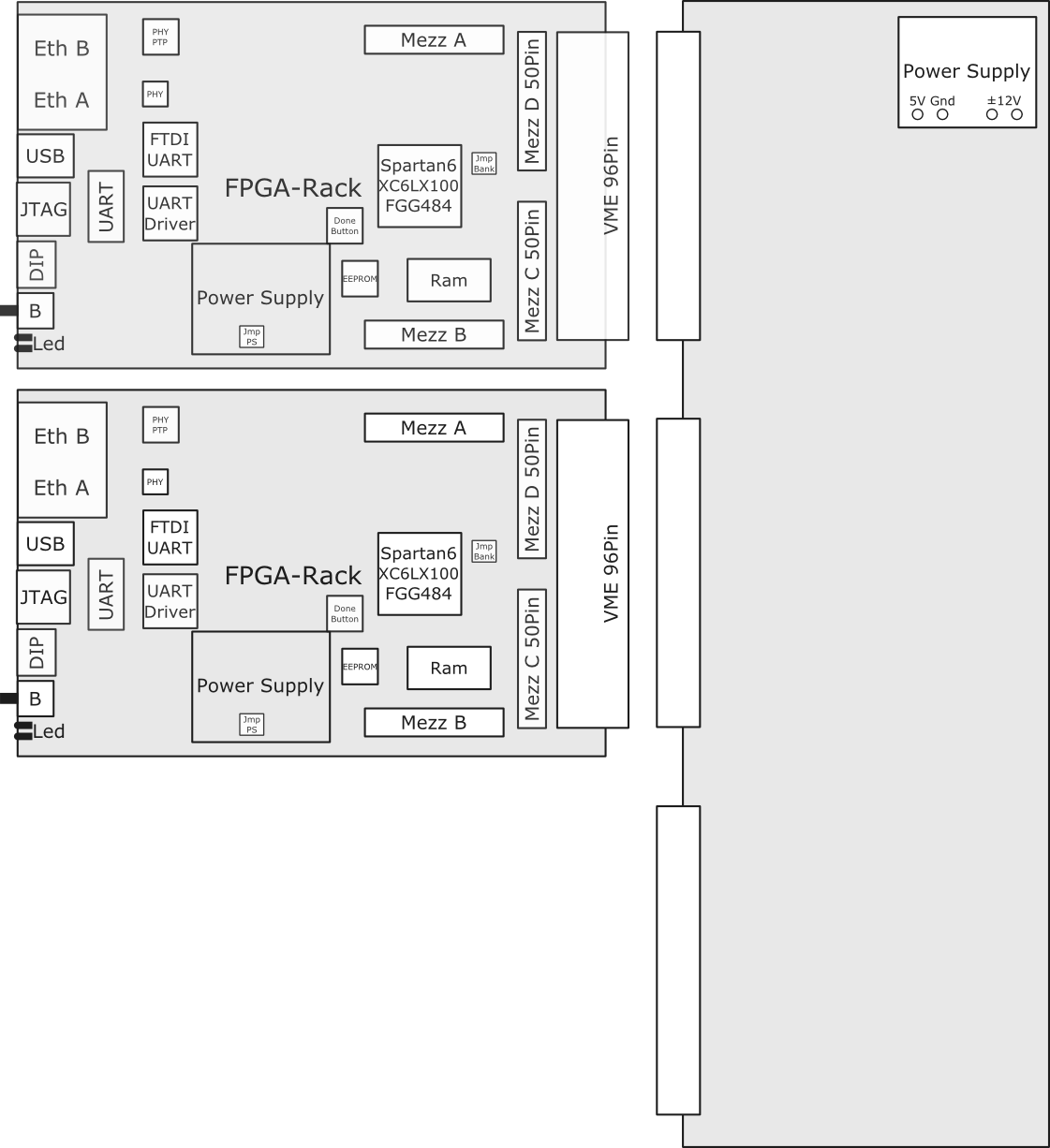
The boards are compatible with the FPGA Rack Backplane for interconnecting different boards with the help of the HES-SO Backplane Bus and the HES-SO VME IP Core.
A VHDL test code with the default UCF Files can be found at the EDA SVN Repository:
Limitation
There are Boards with 3 types of FPGA's on it; XC6SLX45, XC6SLX100 and XC6SLX150.
Leds and Buttons
There are 4 Dil switches and 4 Leds mounted on the FPGARack board. They are not properly indicated 0 - 3 therefore see the image below.
Features
- 2 Port Ethernet (one PTP physical)
- USB FTDI
- 2 UART
- Flash 128Mb - 512Mb
- Ram 128Mb - 256Mb
- Spartan 6 LX45 - LX100 - LX150
- 4 Leds
- 4 Dil Switches
- 1 Button
- 106.25MHz Main Clock
- VME compatible connector 3x32Pin
- 2 Debug connectors 2x50Pin
- 2 Mezzanine Connector ARM-EBS and FPGA-EBS compatible
- Powered by USB or VME Power
VME connector logic levels
The I/O bank which interfaces the VME connector (and the little black connectors) can be powered with 3.3V or with 2.5V. A zero-Ohm resistor has to be soldered at the proper place near the FPGA.
Programmation
This board can be programmed in 2 ways,
- first the FPGA can be directly programmed
- second the FPGA can be programmed via the onboard Flash memory
For more explanation see at the Howto below:

