Hardware/Parallelport/Audio ADC DAC
(Difference between revisions)
m |
m (→Usage) |
||
| Line 16: | Line 16: | ||
== Usage == | == Usage == | ||
| − | This board is used in the "[http://wiki.hevs.ch/fsi/index.php5/EMVs/AudioAmp Filiere Promotions for the EMVS]" | + | This board is used in the "[http://wiki.hevs.ch/fsi/index.php5/EMVs/AudioAmp Filiere Promotions for the EMVS]" Day, where the future students can build a Audio Amplifier Class-D. |
| − | + | ||
== Test == | == Test == | ||
Revision as of 14:11, 22 January 2014
|
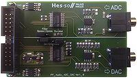
Audio ADC DAC board
The board bases on 2 different chips.
- ADC Chip is a BB PCM1804 full differential analog input 24-BIT, 192-kHz stereo A/D converter.
- DAC Chip is a BB PCM1793 24-BIT, 192kHz Stereo D/A converter.
| Version | Photo | Schematics | Description |
|---|---|---|---|
| V1.0 |  |
Mezza ADC DAC Schematic PDF | ADC & DAC parallelport board |
Both the ADC and DAC Chips are supplied by +5V. These power is generated in two steps from the +3.3V power supply from the FPGA-EBS. In the first step with a steup up from +3.3V to ~+5.5V and in a second step, for the DAC and the ADC separably, a VLDO to +5V.
Usage
This board is used in the "Filiere Promotions for the EMVS" Day, where the future students can build a Audio Amplifier Class-D.
Test
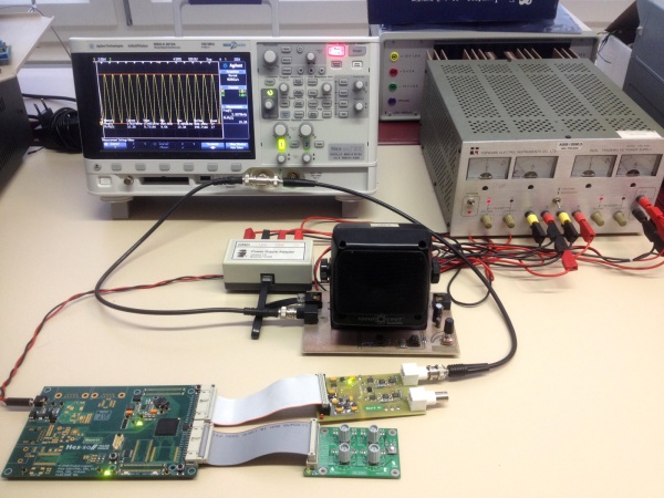
Connect the board to the top connector of an FPGA development board.
Connect a 4-pieces rotary switch board to the lower connector of the FPGA board.
Download the sinewave design.
- Check the power supplies: +12 V, -12 V, +5 V.
- Check the reference voltage: 10 V on pin 6 of the large chip in the middle of the 2 DAC rails.
- Check the digital serial signals on the FPGA board connector (pins TBD).
- Check the raw DAC voltage on the left side of each leftmost resistor.
- Check the voltage outputs of the board.
