Hardware/Parallelport/Audio ADC DAC
From UIT
|
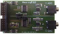
Audio ADC DAC board
The board bases on 2 different chips.
- ADC Chip is a BB PCM1804 full differential analog input 24-BIT, 192-kHz stereo A/D converter.
- DAC Chip is a BB PCM1793 24-BIT, 192kHz Stereo D/A converter.
| Version | Photo | Schematics | Description |
|---|---|---|---|
| V1.0 |  |
Mezza ADC DAC Schematic PDF | ADC & DAC parallelport board |
Both the ADC and DAC Chips are supplied by +5V. These power is generated in two steps from the +3.3V power supply from the FPGA-EBS. In the first step with a steup up from +3.3V to ~+5.5V and in a second step, for the DAC and the ADC separably, a VLDO to +5V.
Usage
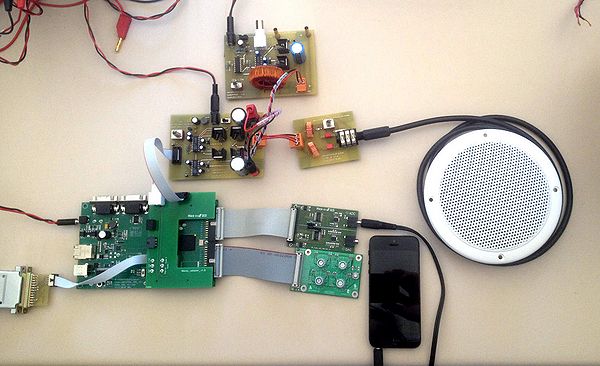
This board is used in the "Filiere Promotions for the EMVS" Day, where the future students can build a Class-D Audio Amplifier.
Projects
- U-SLO
- The DAC links the triangle signal generated by an FPGA to the mirror driver board.
- The ADC converts the signal received from the optical sensor for processing by an FPGA.
Audio Amp Test
- Use FPGA-EBS v2.x
- Connect the AD-DA board via parallel cable
- Connect the Rotary Switch board via parallel cable
- Connect Mezzanine Audio Adapter board
- Power the FPGA via the Mezzanine connector
- Connect Step-Up with a coax cable
- Connect H-Bridge with the 1 Pin parallel cable
- Connect Step-Up with the H-bridge
- Connect H-Bridge with the Lowpass filter for the Loudspeaker
- Connect the Loudspeaker
- Power Step-up and H-Bridge with +12V - Gnd
