Kart/FPGA board
(→Test) |
|||
| (One intermediate revision by one user not shown) | |||
| Line 20: | Line 20: | ||
== Test == | == Test == | ||
| − | A test board routes the FPGA motherboard connector pins from one to the next. | + | A [[Media:Kart tester board.pdf|test board]] routes the FPGA motherboard connector pins |
| + | from one to the next. | ||
The path also includes the SCL and SDA pins of the bus connector. | The path also includes the SCL and SDA pins of the bus connector. | ||
| − | The path | + | The path extremities are located on spare I/Os of the JTAG programming connector. |
| − | Each pair of pins are also connected to a | + | Each pair of pins are also connected to a LED, which shows to what extent the signal path is functional. |
[[File:Kart fpga test board.JPG|center|400px|FPGA motherboard]] | [[File:Kart fpga test board.JPG|center|400px|FPGA motherboard]] | ||
| Line 32: | Line 33: | ||
The system is powered via a circular connector which connects to a 3.3 V regulator. | The system is powered via a circular connector which connects to a 3.3 V regulator. | ||
5 V is a good power voltage candidate. | 5 V is a good power voltage candidate. | ||
| + | |||
| + | == Sniffer == | ||
| + | |||
| + | The RS232 to USB [[Media:Kart USB-RS232 board.pdf|board]] can be used as an FPGA mezzanine | ||
| + | with only the FTDI USB to RS232 chip mounted. | ||
[[Category:Kart]] | [[Category:Kart]] | ||
Latest revision as of 10:33, 3 September 2021
|
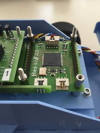
The FPGA motherboards are equipped with an AGL125 IGLOO in a VQ100 package and a 10 MHz Quartz.
Connection
They have two I2C connectors on one side and the programming connector on the other side. The I2C connectors allow daisy chaining either with fixed-length PCBs or with flat cables.
The daughterboards connect on the two single row connectors on the long sides. The mounting screws on 3 corners only are used to secure against placing the daughter board the wrong way round.
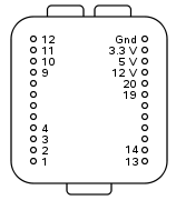
The following figure shows the pinning in case of test needs:
Test
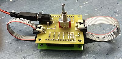
A test board routes the FPGA motherboard connector pins from one to the next. The path also includes the SCL and SDA pins of the bus connector. The path extremities are located on spare I/Os of the JTAG programming connector. Each pair of pins are also connected to a LED, which shows to what extent the signal path is functional.
A square wave is sent from one extermity to the other, thus having half of the pins working as outputs and the other half working as inputs. A switch allows to invert the path's direction, thus changing the I/O mode of all the pins.
The system is powered via a circular connector which connects to a 3.3 V regulator. 5 V is a good power voltage candidate.
Sniffer
The RS232 to USB board can be used as an FPGA mezzanine with only the FTDI USB to RS232 chip mounted.


