Kart/Motherboard
|
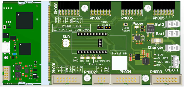
The Kart motherboard will receive any compatible FPGA daughterboard such as the AGLN250 one used during the Kart project and redistribute I/Os. It also powers the system.
Power
The main power entry point of the system is through the motherboard, either by using the two battery connectors with two 6V / 2400mAh packs put in series, or the charger port with a 12V input from a regulated DC supply.
The 12V is then reduced to a 5V rail through a buck converter.
Finally, the daughterboard is fed with the 5V to provide a 3.3V rail.
Charging
The Charger connector is used with a DC supply to test the system, but also for an NiMh charger to be connected.
Make sure to shut the circuit off while charging to avoid higher voltage on the 12V rail.
The charge rate should be of around 0.05C => 120mA here.
Power-on
A switch must be connected to the corresponding port to power the board. The 12V is then transported to the PMODs and the buck converter through a 3A-T fuse.
Please test the circuit with a DC power supply with current limitation capabilities (1 [A] should be far enough while no mechanical constraint is applied on the motors).
If the fuse breaks, check for any short-circuit before replacing it and power-cycling the circuit.
A green LED shows the board power status.
Power state
An I2C dual-inputs ADC converter (MCP3426A0) is present on the board to read both the battery voltage and the current consumption.
Access the data
The chip is read from the FPGA each second through dedicated I2C lines.
The information can be read from the smartphone at will by accessing the corresponding registers.
Daughterboard
The daughterboard is mounted through an SODIMM-200 (DDR2 RAM) connector.
I/Os
PMOD
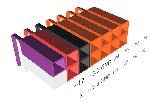
The board allows for multiple I/Os to be plugged following the PMOD wiring, lightly modified for the Kart, under the following form:
- 4 full connectors for direct plug (PMODs 5 to 8)
- 3 full connector for flat-cables (PMODs 1, 3, 4)
- 1 half connector for flat-cable (PMOD 2)
PMOD8 pins 6 to 8 cannot be used with the AGLN250 FPGA. In such case, use the connector on one row (the upper one).
The pins are described on the board itself and correspond to the following:
Two identical motor driver Pmods are furnished. They allow to control the propulsion DC and the steering stepper motors.
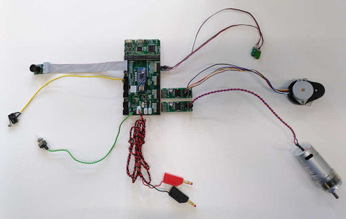
Various sensors can be wired as seen here.
At all time, ensure there is NO VOLTAGE FEEDBACK from anything else than 3.3V on the I/Os. Use a dedicated power board if needed.
The preferred connection is shown in the following picture:
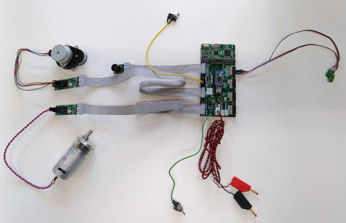
Alternatively, flat cables can be used, as shown in the following picture:
In this case, the I/O constraints file has to be updated !
FPGA reset
A small button allows the user to reset the FPGA from the motherboard.
UART sniffers
Both Tx from the FPGA and the BLE module can be sniffed by wiring a dedicated UART-USB chip to the provided headers.
BLE Socket
The Bluetooth - USB dongle can be inserted in its dedicated socket to control the Kart with a smartphone, or easily removed to be plugged in a PC directly.
One can emulate the BLE module with the help of a custom serial interpreter by simply plugging the daughterboard in a PC through the USB-C. The communication is merged between both the PC and the BLE module.


