Components/IP/NanoBlaze
(→Assembler) |
(→Component) |
||
| Line 4: | Line 4: | ||
[[File:nanoBlaze.png|250px|thumb|right]] | [[File:nanoBlaze.png|250px|thumb|right]] | ||
| − | The '''NanoBlaze''' is a grow-up of the [http://www.xilinx.com/picoblaze.html Xilinx | + | The '''NanoBlaze''' is a grow-up of the [http://www.xilinx.com/picoblaze.html Xilinx PicoBlaze] microcontroller, hence the name. |
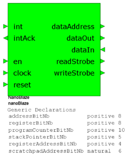
Various sizes can be defined with the help of generic parameters: | Various sizes can be defined with the help of generic parameters: | ||
*<code>registerBitNb</code> defines the data bit width | *<code>registerBitNb</code> defines the data bit width | ||
| Line 15: | Line 15: | ||
With <code>scratchPadAddressBitNb = 0</code>, the scratchpad is not implemented. | With <code>scratchPadAddressBitNb = 0</code>, the scratchpad is not implemented. | ||
| + | |||
| + | The NanoBlaze's instruction ROM is designed to be mapped as a Block RAM. | ||
| + | |||
| + | Contrarily to the PicoBlaze, the NanoBlaze performs every instruction within a single clock cycle. | ||
| + | Due to the mapping of the instruction ROM into a Block RAM, the instructions are provided delayed by one clock period compared to the program counter. | ||
| + | With this, when a branch condition is met, the processor will anyway receive the instruction of the next memory location. | ||
| + | Obviously, this instruction will not be executed, but this means that every successful branch requires two clock cycles. | ||
= Assembler = | = Assembler = | ||
Revision as of 17:01, 8 April 2015
|
Component
The NanoBlaze is a grow-up of the Xilinx PicoBlaze microcontroller, hence the name. Various sizes can be defined with the help of generic parameters:
registerBitNbdefines the data bit widthprogramCounterBitNballows to cope with different program lengthsstackPointerBitNbadapts to various nesting depths of the subroutinesregisterBitNbdefines the data bit widthregisterAddressBitNballows to choose the number of internal registersscratchPadAddressBitNballows to manage the size of the scratchpadaddressBitNbdefines the size of the I/O space
With scratchPadAddressBitNb = 0, the scratchpad is not implemented.
The NanoBlaze's instruction ROM is designed to be mapped as a Block RAM.
Contrarily to the PicoBlaze, the NanoBlaze performs every instruction within a single clock cycle. Due to the mapping of the instruction ROM into a Block RAM, the instructions are provided delayed by one clock period compared to the program counter. With this, when a branch condition is met, the processor will anyway receive the instruction of the next memory location. Obviously, this instruction will not be executed, but this means that every successful branch requires two clock cycles.
Assembler
It has an assembler written in PERL which runs on any operating system. With this, the assembler can easily be integrated in the Mentor HDL Designer environment.
The VHDL processor code includes a disassembler process which writes the current instruction in the form of a string.
This string can be displayed in the simulator for debugging purpose.
The corresponding VHDL code is commented out for synthesis via the pragma translate_off clause.
Sources
This IP is found in the HEVs EDA Repository: svn: https://repos.hevs.ch/svn/eda/
