Hardware/FPGARack4ethernet
(Difference between revisions)
| Line 12: | Line 12: | ||
The board is compatible with the [[Hardware/FPGARackBackplane|FPGA Rack Backplane]] for interconnecting different boards with the help of the [[Standards/HEVs_'VME'_Backplane_Bus|HES-SO Backplane Bus]] and the [[Components/IP/VME|HES-SO VME IP Core]]. | The board is compatible with the [[Hardware/FPGARackBackplane|FPGA Rack Backplane]] for interconnecting different boards with the help of the [[Standards/HEVs_'VME'_Backplane_Bus|HES-SO Backplane Bus]] and the [[Components/IP/VME|HES-SO VME IP Core]]. | ||
| + | |||
| + | = PHY clocks = | ||
| + | |||
| + | All 4 PHYs receive the same 25 MHz clock. | ||
| + | This clock signal can be sourced from: | ||
| + | * the quartz oscillator closest to the PHYs (<code>CLK_PHY_25M</code>) | ||
| + | * the FPGA (<code>CLK_PHY_FPGA</code>, pin AB13). | ||
| + | |||
| + | The FPGA can generate the PHY clock from | ||
| + | * a 106.25 MHz quartz (<code>CLK_106_25M</code>, pin Y13) | ||
| + | * the PHY quartz oscillator (<code>CLK_PHY_25M</code>, pin AA12) | ||
| + | * one of the PHY Rx or Tx clocks (<code>ETHA_RX_CLK</code>, <code>ETHA_TX_CLK</code>, <code>ETHB_RX_CLK</code>, …) | ||
| + | |||
| + | The last possibility is foreseen to [https://en.wikipedia.org/wiki/Synchronous_Ethernet synchronise] the clocks of slave Ethernet ports to the one of a master port. | ||
<!-- | <!-- | ||
Revision as of 17:30, 11 January 2016
|
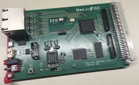
This board is a variant of the FPGA rack board, but with 4 Ethernet connectors.
| Type | FPGA Rack | Schematic | UCF | Description |
|---|---|---|---|---|
| V1.0 |  |
FPGA-Rack-Ethernet4 v1.0 Schematic PDF | FPGA-Rack v1.0 UCF Files | There are different FPGA mounted: Spartan 6 XC6SLX45, Spartan 6 XC6SLX100, Spartan 6 XC6SLX150 |
The board is compatible with the FPGA Rack Backplane for interconnecting different boards with the help of the HES-SO Backplane Bus and the HES-SO VME IP Core.
PHY clocks
All 4 PHYs receive the same 25 MHz clock. This clock signal can be sourced from:
- the quartz oscillator closest to the PHYs (
CLK_PHY_25M) - the FPGA (
CLK_PHY_FPGA, pin AB13).
The FPGA can generate the PHY clock from
- a 106.25 MHz quartz (
CLK_106_25M, pin Y13) - the PHY quartz oscillator (
CLK_PHY_25M, pin AA12) - one of the PHY Rx or Tx clocks (
ETHA_RX_CLK,ETHA_TX_CLK,ETHB_RX_CLK, …)
The last possibility is foreseen to synchronise the clocks of slave Ethernet ports to the one of a master port.