Inverter
|
The Filière Energie et Techniques environnementales (FET) has the digital systems course and labs in the 3rd (autumn) semester. The semester counts 15 weeks and ends with a little project. The aim of the inverter project is to generate a 50 Hz AC power supply from a DC input.
Specification
Function
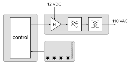
The 12 V power supply is chopped by the power switches of an H-bridge in order to generate a sine wave. The resulting voltage is filtered by a passive LC filter to provide a smooth sine wave. The digital system generates the PWM controls of the 4 power switches.
An I/O board with 4 switches and 8 LEDs allows to control the operating mode and to display information about the system's state.
Output
The system has to generate a 110 VAC power supply.
This is achieved with the help of a transformer. This transformer:
- provides ah high enough voltage amplitude to allow the generation of a 110 VAC output from a 12 power supply
- transforms a differential signal into a floating one, allowing a simple measurement.
As the output voltage is high, great care has to be taken with the transformer output side.
Components
The system consists of
FPGA board
The main board is the school's FPGA-EBS lab development board. It hosts a Xilinx Spartan xc3s500e FPGA and features many different interfaces. The clock oscillates at 66 MHz.
Inverter board
H-bridge
The H-bridge board is powered with 12 V. The 4 IRF7809 MOS transistors are driven by 2 IR2113S driver circuits. The dead time between the switching of the upper and lower part of an H-bridge branch must be greater then 200 ns.
In order for the dead time effect to be negligible, the PWM period will be chosen to be in the order of magnitude off 100 times longer thant the dead time itself. The PWM controls are brought to the inverter board via a ribbon cable.
The 12 V power supply from this board is brought to a 5 V regulator and from there to a connector. From this connector, a cable is used to power the FPGA board as well.
LC lowpass
The LC lowpass is used in conjunction with the H-bridge. It smooths the PWM signal into a sine wave.
The LC cutoff frequency is something like 100 Hz.
Transformer
The transformer allows to reference the differential output to any common voltage.
The board at our disposal transforms 12 V to xxx V (TBD). As it provides a high voltage, it should be handled with great care.
Logic-level LC lowpass
The logic-level LC lowpass board is used to verify the content of the PWM signals in the two H-bridge branches. It smooths the two FPGA output PWM signals into the components of a differential sine wave.
For this lowpass, the default LC cutoff frequency is close to 20 kHz.
Buttons and LEDs I/O board
The buttons and LEDs board is used in conjunction with the FPGA board.
It has 4 buttons and 8 LEDs. It can hold an optional LCD display.
Getting started
In order to start the projects you should do the following:
- Read carefully the specifications above
- Draw the architecture of the circuit in the form of a block diagram
- Consult the guides for the first steps into the design software
PWM modes
Different PWM modes can be investigated:
- a two-level mode with inverted controls on each H-bridge branch
- three-level modes with separate controls on each branch
The PWM modes are further explained in the following sections:
Additional Information
- Board combinations
- Additional informations for teachers.

