Hardware/Parallelport/DAC2
From UIT
|
Two-Channel DAC board
The board bases on 2 AD5543 16-bit DACs. The DACs have a serial input (CS, CLK, SDI) and can be operated up to 3 MHz sampling rate with 0.5 µs settling time.
| Version | Photo | Schematics | Description |
|---|---|---|---|
| V1.0 |  |
HEB DAC Schematic PDF | 2-Channel DAC parallelport board |
The DACs have a current output and a first op-amp converts the currents to voltages. A second op-amp allows to set an offset and a gain with the help of resistors placed in through-hole pins.
The DACs are supplied with +5 V. The op-amps are supplied with ±12 V. These power supplies are generated from the parallel port connector's 3.3 V.
Test
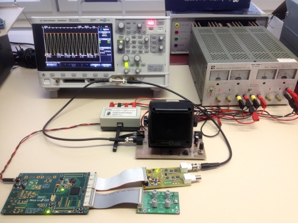
Connect the board to the top connector of an FPGA development board.
Connect a 4-pieces rotary switch board to the lower connector of the FPGA board.
Download the sinewave design.
- Check the power supplies: +12 V, -12 V, +5 V.
- Check the reference voltage: 10 V on pin 6 of the large chip in the middle of the 2 DAC rails.
- Check the digital serial signals on the FPGA board connector (pins TBD).
- Check the raw DAC voltage on the left side of each leftmost resistor.
- Check the voltage outputs of the board.
