Hardware/Parallelport/heb inverter
From UIT
|
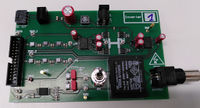
Inverter board
The board was designed for the ETE ELN-inverter lab.
It receives 4 PWM signals to drive an H-Bridge. The bridge is followed by an LC-lowpass and a transformer.
A sigma-delta ADC reads the LC filter output and enables to adjust the output voltage.
| Version | Photo | Schematics | Stock |
|---|---|---|---|
| V1.0 |  |
HEB-inverter Schematic PDF | 16fully mounted |
Dead time
The dead time estimation for the H-Brige has been setimated by augmenting it an monitoring the power consumption of the system. The daead time was given by a counter clocked at 66 MHZ, but with a different number of bits for each measure.
| bit nb | dead time [ns] | current [mA] |
|---|---|---|
| 3 | 121 | 860 |
| 4 | 242 | 170 |
| 5 | 485 | 75 |
| 5 | 970 | 70 |