Hardware/FPGARack
(Difference between revisions)
m |
m |
||
| Line 3: | Line 3: | ||
The basic idea behind this board is to have a development FPGA board, with a choice of big FPGA's and a VME compatible 2U Rack connector. | The basic idea behind this board is to have a development FPGA board, with a choice of big FPGA's and a VME compatible 2U Rack connector. | ||
| − | + | = Freatures = | |
* 2 Port Ethernet | * 2 Port Ethernet | ||
* USB FTDI | * USB FTDI | ||
| Line 30: | Line 30: | ||
* https://repos.hevs.ch/svn/eda/VHDL/FPGARack | * https://repos.hevs.ch/svn/eda/VHDL/FPGARack | ||
| − | + | = Programmation = | |
This board can be programmed in 2 ways, | This board can be programmed in 2 ways, | ||
* first the FPGA can be directly programmed | * first the FPGA can be directly programmed | ||
| Line 38: | Line 38: | ||
* [[Hardware/FPGARack/Programmation|FPGA Rack Programmation]] | * [[Hardware/FPGARack/Programmation|FPGA Rack Programmation]] | ||
| − | = | + | = Links = |
| − | + | * [http://www.xilinx.com/support/documentation/spartan-6.htm Xilinx Spartan 6 Documents] | |
| − | + | * [http://de.wikipedia.org/wiki/VMEbus VME] Connector [http://www.interfacebus.com/Design_Connector_VME.html Description] | |
| − | + | ||
| − | + | ||
| − | + | ||
| − | + | ||
| − | * | + | |
| − | + | ||
| − | + | ||
| − | + | ||
| − | + | ||
** VME or IEEE 1014-1987 (96Pin; 3*32Pin) | ** VME or IEEE 1014-1987 (96Pin; 3*32Pin) | ||
*** [http://www.interfacebus.com/VME_P1_Connector_Pinout.html VME P1] | *** [http://www.interfacebus.com/VME_P1_Connector_Pinout.html VME P1] | ||
*** [http://www.interfacebus.com/VME_P2_Connector_Pinout.html VME P2] | *** [http://www.interfacebus.com/VME_P2_Connector_Pinout.html VME P2] | ||
| − | |||
| − | |||
| − | |||
| − | |||
| − | |||
| − | |||
| − | |||
| − | |||
| − | |||
| − | |||
| − | |||
| − | |||
| − | |||
| − | |||
| − | |||
| − | |||
| − | |||
| − | |||
| − | |||
| − | |||
[[File:fpga_rack_system.png|FPGA Rack System]] | [[File:fpga_rack_system.png|FPGA Rack System]] | ||
[[Category:Hardware]] [[Category:FPGARack]] | [[Category:Hardware]] [[Category:FPGARack]] | ||
Revision as of 09:02, 21 June 2012
|
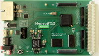
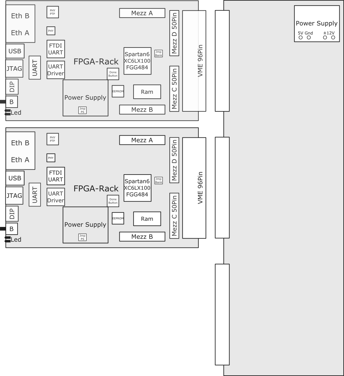
The basic idea behind this board is to have a development FPGA board, with a choice of big FPGA's and a VME compatible 2U Rack connector.
Freatures
- 2 Port Ethernet
- USB FTDI
- 2 UART
- Flash 128Mb - 512Mb
- Ram 128Mb - 256Mb
- Spartan 6 LX45 - LX100 - LX150
- 4 Leds
- 4 Dil Switches
- 1 Button
- 106.25MHz Main Clock
- VME compatible connector 3x32Pin
- 2 Debug connectors 2x50Pin
- 2 Mezzanine Connector ARM-EBS and FPGA-EBS compatible
- Powered by USB or VME Power
| Type | FPGA Rack | Schematic | UCF | Description |
|---|---|---|---|---|
| V1.0 |  |
FPGA-Rack v1.0 Schematic PDF | FPGA-Rack v1.0 UCF Files | There are different FPGA mounted: Spartan 6 XC6SLX45, Spartan 6 XC6SLX100, Spartan 6 XC6SLX150 |
A VHDL test code with the default UCF Files can be found at the EDA SVN Repository:
Programmation
This board can be programmed in 2 ways,
- first the FPGA can be directly programmed
- second the FPGA can be programmed via the onboard Flash memory
For more explanation see at the Howto below:
Links
- Xilinx Spartan 6 Documents
- VME Connector Description
