Hardware/FPGARack
|
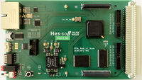
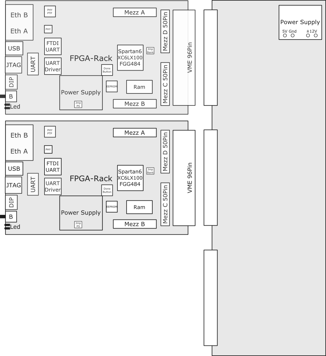
The basic idea behind this board is to have a development FPGA board, with a choice of big FPGA's and a VME compatible 2U Rack connector. The stock can be verified and updated on-line.
| Type | FPGA Rack | Schematic | UCF | Description |
|---|---|---|---|---|
| V1.0 |  |
FPGA-Rack v1.0 Schematic PDF | FPGA-Rack v1.0 UCF Files | There are different FPGA mounted: Spartan 6 XC6SLX45, Spartan 6 XC6SLX100, Spartan 6 XC6SLX150 |
The boards are compatible with the FPGA Rack Backplane for interconnecting different boards with the help of the HES-SO Backplane Bus and the HES-SO VME IP Core.
A VHDL test code with the default UCF Files can be found at the EDA SVN Repository:
Limitation
There are Boards with 3 types of FPGA's on it; XC6SLX45, XC6SLX100 and XC6SLX150.
Leds and Buttons
There are 4 Dil switches and 4 Leds mounted on the FPGARack board. They are not properly indicated 0 - 3 therefore see the image below.
Features
- 2 Port Ethernet (one PTP physical)
- USB FTDI
- 2 UART
- Flash 128Mb - 512Mb
- Ram 128Mb - 256Mb
- Spartan 6 LX45 - LX100 - LX150
- 4 Leds
- 4 Dil Switches
- 1 Button
- 106.25MHz Main Clock
- VME compatible connector 3x32Pin
- 2 Debug connectors 2x50Pin
- 2 Mezzanine Connector ARM-EBS and FPGA-EBS compatible
- Powered by USB or VME Power
VME connector logic levels
The I/O bank which interfaces the VME connector (and the little black connectors) can be powered with 3.3V or with 2.5V. A zero-Ohm resistor has to be soldered at the proper place near the FPGA.
Programmation
This board can be programmed in 2 ways,
- first the FPGA can be directly programmed
- second the FPGA can be programmed via the onboard Flash memory
For more explanation see at the Howto below:

