Components/IP/VME
|
The HES-SO VME IP Core was designed within the project BasMI. Is is used in the VME Backplanes for interconnecting different Rack Boards together. This IP can be found on the EDA Repository: svn: https://repos.hevs.ch/svn/eda/
Introduction
At the moment of the creation of this document, some new FPGA development cards have been realized at the HES-SO Valais/Wallis Sion. There are the FPGA Rack V1 board (successor of the old FPGA-EBS, for general purpose) and the FPGARack AD/DA V1 board (initially done for the OLGM project).
These new PCBs have Eurocard (100x160mm) size and a DIN41612 3x32pin connector soldered. So, this document describes the work realized around this new communication bus (physical and VHDL). The goal was to define and create the communication in the aforementioned DIN41612 conncetor. It was choosen to create a modified VME Bus called HVME (HES-SO VME).
Compatible Rack Boards
Available Rack Backplanes
Bus Specification
VHDL Implementation
Two controllers (master and slave) have been realized and are available in the EDA repository inside the VME library - with dependency to EDAC and Memory libraries.
Master Controller
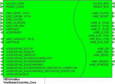
The master controller is available under the name “VmeMasterController_Core”.
The first side, clocked at the core clock iCLOCK_CORE, offers to the user an input FIFO for all read/write requests (i/oCMD*) and a direct output for incoming slave read data (oRET*). Debugs signals are available for identify potential problems on the bus, like freezing (oDEBUGFLAG*). Let’s just take an example: you want to read data on the bus. The procedure is the following :
- Place the command request on all iCMD_* signals, where:
- iCMD_ADDR is the address (right justified for 16bit device).
- iCMD_DATAIN is the data to write (right justified for 16bit device).
- iCMD_ECCEN enable the ECC management for this bus access (0: enabled, 1: disabled).
- iCMD_SLVMODE set the access mode (0: 16bit, 1: 32bit).
- iCMD_WR_RDn define if it’s a read (0) or write (1) operation. </br>The validation of the command has to be done by setting high iCMDVALID (only if oCMDREADY is high!). These requests can be bursted, because they are accumulated into a FIFO. If the FIFO is full (-1), it causes oCMDREADY signal to rise.
- The controller processes the request during an undetermined time (depending on the FIFO occupation and ECC transmission error)...
- When the oRETVALID is high, consume the slave data on oRET_DATAOUT.
Writing operation is similar, excepting no data are returned.
On the other side (the VME bus control) is clocked to iCLOCK_BUS – generally generated by a PLL consuming the core clock. All signals should be routed to the corresponding physical lines (VME_D, VME_ECC and VME_sReady must be “tristated” on top).
Three integer generics can be configured:
-
gTXFifo_AddrWidth: Set the FIFO width for storing the incoming command requests. Resulting available cases are 2gTXFifo_AddrWidth-1.
-
gWatchdog_CounterWidth: Number of iCLOCK_BUS cycles (during MFreeze or SReady are high, respectively, low) before give a bus frozen warning via oDEBUGFLAG_ECCREADERROR_WATCHDOG_OVERFLOW / SLAVEWAITREQ_WATCHDOG_OVERFLOW.
-
gSyncStageCount: Number of stages for cross-domain data synchronization.
The master core uses two different clock inputs. On is the user accessible clock iCLOCK_CORE for the CMD and the RET signal interface. The other Clock input is used for the VME bus. The iCLOCK_CORE clock input is used to the logic and is also directly assigned to the oVME_CLOCK, it sets the overall VME clock speed.
Slave Controller
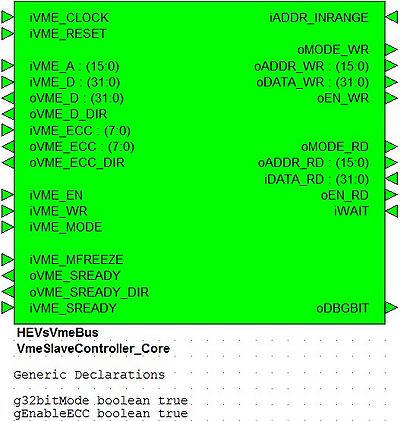
The slave controller is available under the name “VmeSlaveController_Core”.
The left side is connected physically to the HVME bus and consumes its clock. The ECC, Data and sReady lines need to be tristate on board level.
The second size has two groups. In all cases, when an R/W request is present on the bus, its address is on both signals oADDR_WR and oADDR_RD, in addition to oMODE_WR and oMODE_RD. The o*_RD signals are asynchronous, unlike the o*_WR signals (latenced of one cycle for circuitry speed enhancement). Asynchronously, the signals oADDR_RD and oMODE_RD must be decoded and the signal iADDR_INRANGE set if the address is in the range of the specified board. Obviously, each board needs to have a different read address mapping and can’t conflict with a different board – for write address mapping this is not an issue.
For write operation, oADDR_WR and oDATA_WR must be used for write data into register, memory, etc. when oEN_WR is high (iADDR_INRANGE is already considered on it).
Similarly for a read operation, when oEN_RD is high, the data pointed by oADDR_RD must be placed on iDATA_RD, but asynchronously. When the iWAIT signal is set, it freezes the bus via SReady (useful for reading with latency cycles). But please keep in mind that this function has not been tested yet.
oDBGBIT is just a dummy bit for avoiding name/signal simplification on the poor Xilinx ChipScopePro debugger software. If you want to use it, route this to an unused output, otherwise just ignore it.
Two Boolean generics are to consider for configure the controller:
-
g32bitMode: If true, enables the 32bit mode. Otherwise, the controller acts as a 16bit device. This generic as a capital importance in the ECC encode/decode behaviour.
-
gEnableECC: If true, enables the ECC management.
The slave controller uses only one clock inputs. It is the VME bus mclk signal called iVME_CLOCK which can have, depending on the system, different kind of speeds, but normally <20MHz. This means that the user accessible signals are all clocked with with the mentioned mclk. If the system is not powered by the same clock an additional sync_stage between the two clocks is needed.
Slave Controller (with premapped registers)
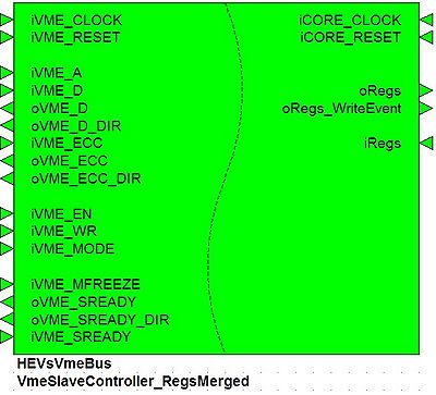
This controller is a simplified core for the user, it is embedding a “VmeSlaveController_Core” and offers to the user a direct access to some registers.
Write registers (stored into the controller) are accessible on the output oRegs (row-major linearized). A write event on any register induces a pulse on its corresponding bit on oRegs_WriteEvent.
User’s read registers must be routed to the iRegs (row-major linearized, again).
Please note that the register side works at the core clock speed (iCORE_CLOCK).
The register in/outputs are arrays of a std_ulogic_vector. One register has either 16 or 32 bit depending on the bitMode generic.
Hereafter the generics to configure this controller:
-
g32bitMode: If true, enables the 32bit mode. Otherwise, the controller acts as an 16bit device. This generic as a capital importance in the ECC encode/decode behaviour.
-
gEnableECC: If true, enables the ECC management.
-
gRegRdAddrWidth: 2gRegWrAddrWidth is the number of user read registers.
-
gRegWrAddrWidth: 2gRegWrAddrWidth is the number of user write registers.
-
gAddressMask: The address mask to apply for evaluating the in-range condition.
-
gAddressValue: The value compared to the masked address for evaluate the in-range condition
For the address range configuration, let’s consider the following example:
| Slave | Address Range | Address Mask | Address Value |
|---|---|---|---|
| Slave A | 0x0000 - 0x0FFF | 0xF000 | 0x0000 |
| Slave B | 0x1000 - 0x1FFF | 0xF000 | 0x1000 |
| Slave C | 0x8000 - 0x9FFF | 0xE000 | 0x8000 |
| Slave D | 0xA000 - 0xBFFF | 0xE000 | 0xA000 |
This slave controller contains the in the aforementioned Slave controller (Core) within. The advantage is that this controller already contains the registers for clock domain crossing within. Hence the additional clock input called iCORE_CLOCK, which has to be bigger than the iVME_CLOCK.
TestBench
TODO


